- 您现在的位置:买卖IC网 > Sheet目录3873 > PIC16F627-04/P (Microchip Technology)IC MCU FLASH 1KX14 COMP 18DIP
PIC16F62X
DS40300C-page 16
Preliminary
2003 Microchip Technology Inc.
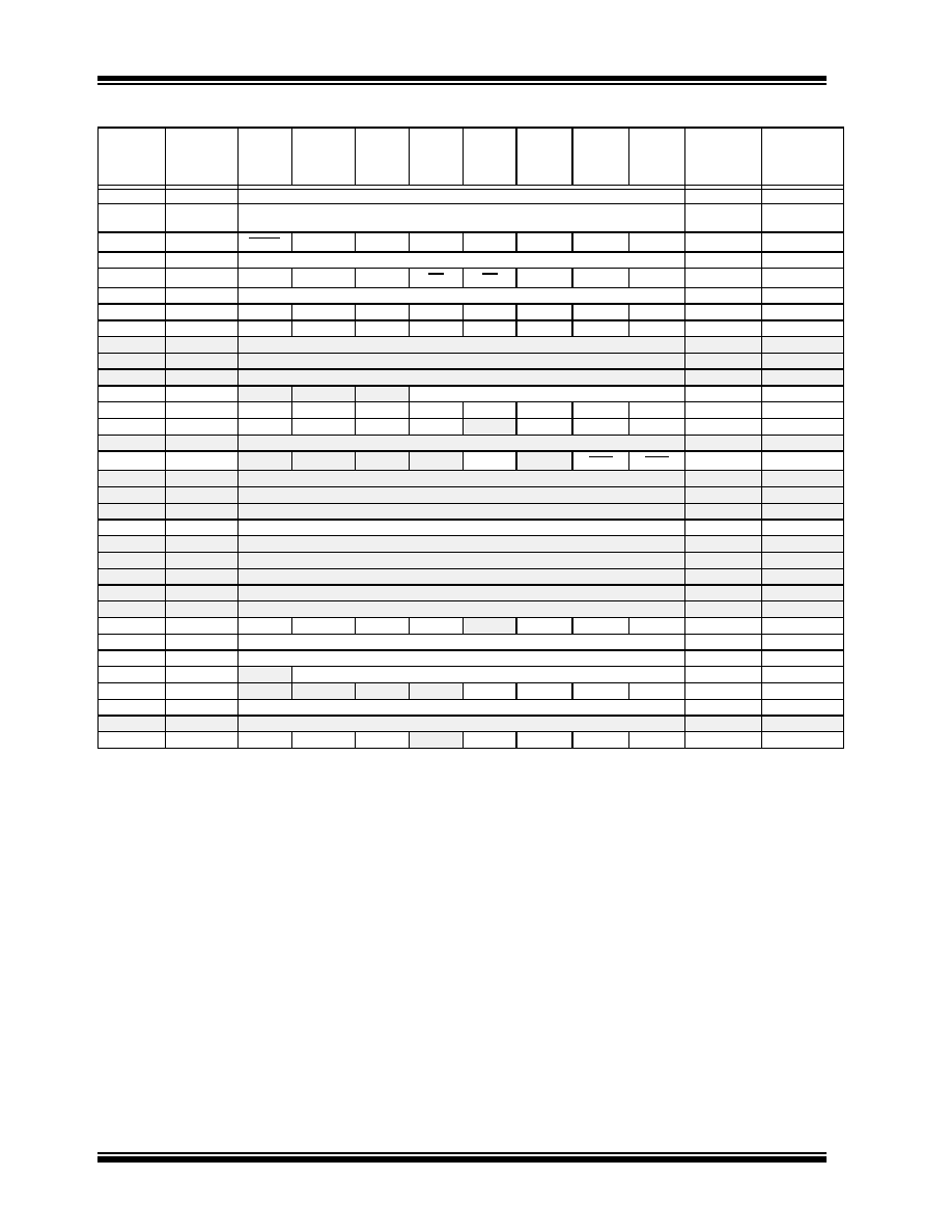
TABLE 3-2:
SPECIAL FUNCTION REGISTERS SUMMARY BANK 1
Address
Name
Bit 7
Bit 6
Bit 5
Bit 4
Bit 3
Bit 2
Bit 1
Bit 0
Value on
POR
Reset(1)
Details on
Page
Bank 1
80h
INDF
Addressing this location uses contents of FSR to address data memory (not a physical
register)
xxxx xxxx
81h
OPTION
RBPU
INTEDG
T0CS
T0SE
PSA
PS2
PS1
PS0
1111 1111
82h
PCL
Program Counter's (PC) Least Significant Byte
0000 0000
83h
STATUS
IRP
RP1
RP0
TO
PD
ZDC
C
0001 1xxx
84h
FSR
Indirect data memory address pointer
xxxx xxxx
85h
TRISA
TRISA7
TRISA6
TRISA5
TRISA4
TRISA3
TRISA2
TRISA1
TRISA0
1111 1111
86h
TRISB
TRISB7
TRISB6
TRISB5
TRISB4
TRISB3
TRISB2
TRISB1
TRISB0
1111 1111
87h
—
Unimplemented
—
88h
—
Unimplemented
—
89h
—
Unimplemented
—
8Ah
PCLATH
—
Write buffer for upper 5 bits of program counter
---0 0000
8Bh
INTCON
GIE
PEIE
T0IE
INTE
RBIE
T0IF
INTF
RBIF
0000 000x
8Ch
PIE1
EEIE
CMIE
RCIE
TXIE
—
CCP1IE
TMR2IE
TMR1IE
0000 -000
8Dh
—
Unimplemented
—
8Eh
PCON
—
OSCF
—POR
BOD
---- 1-0x
8Fh
—
Unimplemented
—
90h
—
Unimplemented
—
91h
—
Unimplemented
—
92h
PR2
Timer2 Period Register
1111 1111
93h
—
Unimplemented
—
94h
—
Unimplemented
—
95h
—
Unimplemented
—
96h
—
Unimplemented
—
97h
—
Unimplemented
—
98h
TXSTA
CSRC
TX9
TXEN
SYNC
—
BRGH
TRMT
TX9D
0000 -010
99h
SPBRG
Baud Rate Generator Register
0000 0000
9Ah
EEDATA
EEPROM data register
xxxx xxxx
9Bh
EEADR
—
EEPROM address register
xxxx xxxx
9Ch
EECON1
—
WRERR
WREN
WR
RD
---- x000
9Dh
EECON2
EEPROM control register 2 (not a physical register)
--------
9Eh
—
Unimplemented
—
9Fh
VRCON
VREN
VROE
VRR
—
VR3
VR2
VR1
VR0
000- 0000
Legend:
— = Unimplemented locations read as ‘0’, u = unchanged, x = unknown, q = value depends on condition, shaded = unim-
plemented
Note
1: For the Initialization Condition for Registers Tables, refer to Table 14-7 and Table 14-8 on page 98.
发布紧急采购,3分钟左右您将得到回复。
相关PDF资料
PIC18F45J10-I/ML
IC PIC MCU FLASH 16KX16 44QFN
PIC18F24K22-I/ML
IC PIC MCU 16KB FLASH 28QFN
PIC16CR76-I/SS
IC PIC MCU 8KX14 28SSOP
PIC16F887-I/P
IC PIC MCU FLASH 8KX14 40DIP
PIC16CR76-I/SP
IC PIC MCU 8KX14 28DIP
PIC16CR76-I/SO
IC PIC MCU 8KX14 28SOIC
PIC16CR76-I/ML
IC PIC MCU 8KX14 28QFN
PIC16CR74T-I/ML
IC PIC MCU 4KX14 44QFN
相关代理商/技术参数
PIC16F627-04/P
制造商:Microchip Technology Inc 功能描述:IC 8BIT FLASH MCU 16F627 DIP18
PIC16F627-04/SO
功能描述:8位微控制器 -MCU 1.75KB 224 RAM 16I/O 4MHz SOIC18 RoHS:否 制造商:Silicon Labs 核心:8051 处理器系列:C8051F39x 数据总线宽度:8 bit 最大时钟频率:50 MHz 程序存储器大小:16 KB 数据 RAM 大小:1 KB 片上 ADC:Yes 工作电源电压:1.8 V to 3.6 V 工作温度范围:- 40 C to + 105 C 封装 / 箱体:QFN-20 安装风格:SMD/SMT
PIC16F627-04/SO
制造商:Microchip Technology Inc 功能描述:8BIT FLASH MCU SMD 16F627 SOIC18
PIC16F627-04/SO
制造商:Microchip Technology Inc 功能描述:Microcontroller IC Number of I/Os:16
PIC16F627-04/SS
功能描述:8位微控制器 -MCU 1.75KB 224 RAM 16I/O 4MHz SSOP20 RoHS:否 制造商:Silicon Labs 核心:8051 处理器系列:C8051F39x 数据总线宽度:8 bit 最大时钟频率:50 MHz 程序存储器大小:16 KB 数据 RAM 大小:1 KB 片上 ADC:Yes 工作电源电压:1.8 V to 3.6 V 工作温度范围:- 40 C to + 105 C 封装 / 箱体:QFN-20 安装风格:SMD/SMT
PIC16F627-04E/P
功能描述:8位微控制器 -MCU 1.75KB 224 RAM 16I/O RoHS:否 制造商:Silicon Labs 核心:8051 处理器系列:C8051F39x 数据总线宽度:8 bit 最大时钟频率:50 MHz 程序存储器大小:16 KB 数据 RAM 大小:1 KB 片上 ADC:Yes 工作电源电压:1.8 V to 3.6 V 工作温度范围:- 40 C to + 105 C 封装 / 箱体:QFN-20 安装风格:SMD/SMT
PIC16F627-04E/SO
功能描述:8位微控制器 -MCU 1.75KB 224 RAM 16I/O 4MHz Ext Temp SOIC18 RoHS:否 制造商:Silicon Labs 核心:8051 处理器系列:C8051F39x 数据总线宽度:8 bit 最大时钟频率:50 MHz 程序存储器大小:16 KB 数据 RAM 大小:1 KB 片上 ADC:Yes 工作电源电压:1.8 V to 3.6 V 工作温度范围:- 40 C to + 105 C 封装 / 箱体:QFN-20 安装风格:SMD/SMT
PIC16F627-04E/SS
功能描述:8位微控制器 -MCU 1.75KB 224 RAM 16I/O 4MHz Ext Temp SSOP20 RoHS:否 制造商:Silicon Labs 核心:8051 处理器系列:C8051F39x 数据总线宽度:8 bit 最大时钟频率:50 MHz 程序存储器大小:16 KB 数据 RAM 大小:1 KB 片上 ADC:Yes 工作电源电压:1.8 V to 3.6 V 工作温度范围:- 40 C to + 105 C 封装 / 箱体:QFN-20 安装风格:SMD/SMT